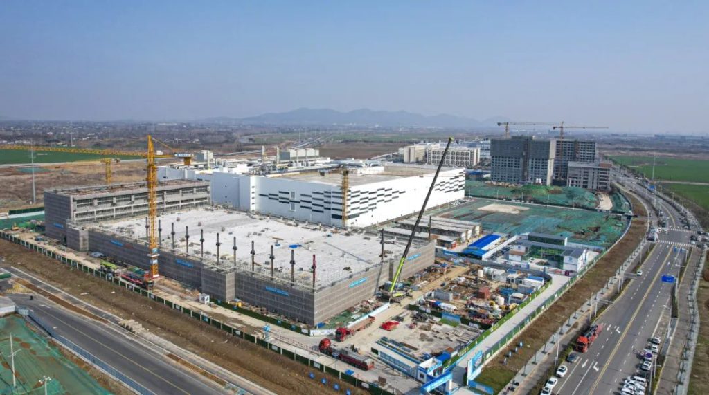
Jiangsu Huatian wafer-level advanced packaging and testing production line projectLocated in Pukou Economic Development Zone. Now, a huge plant has taken shape, and inside and outside the building, workers are busy - boarding trucks, car cranes, lift trucks, and hanging baskets, all on line to speed up the construction progress.The project, with a total investment of 9.95 billion yuan, will be constructed in three phases, with the current topping out being the first phase.Upon completion, it will be a Class 100 clean plant production line to meet the business needs of wafer-level packaging, wafer-level bump packaging, high-density fan-out packaging, and high-pixel image sensor packaging.
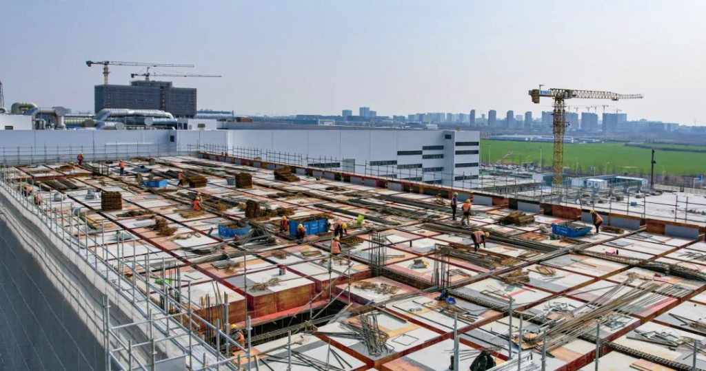
"Chip sealing and testing of space cleanliness requirements are very high." Construction unit China Construction Bureau Jiangsu Branch project manager introduced, general hospital ICU sterilization and disinfection with reference to the 100,000 level standard, while the Nanjing IC wafer-level advanced sealing and testing production line project to reach a hundred level. The lower the number represents the number of particles in the air the less, the higher the purification level, which also means that the plant clean area standards than the ICU standard is also high. And in order to achieve this goal, the project innovatively adopts high-precision Chi-Chi plate construction technology, Chi-Chi plate structure consists of Chi-Chi barrels and reinforced concrete.
The 3-story floor slab of over 10,000 square meters is densely packed with more than 26,000 holes with a diameter of 39 centimeters, ensuring that air circulates and circulates through the holes and is purified in a timely manner. The main body of the project is a steel frame structure with a maximum span of 40 meters in a single bay. The construction unit used a 350-ton crawler crane to lift across the outside, picking up the "strongest back" of the industrial plant.
Huatian Technology is one of the top 10 global sealing and testing companies, and the company has continued to increase its capital since it settled in Nanjing in 2018.Wafer-level advanced sealing and testing production line since October last year, to this month's full topping out in just over seven months.It is reported that the project is scheduled to be completed and put into operation in June, after the completion of the overall project, with a wafer-level packaging capacity of 700,000 pieces of the expected annual sales revenue of 7 billion yuan, Nanjing to promote the "new quality" project to accelerate the landing of a microcosm.
subocular (medicine)
Pukou Economic Development Zone
Continuously promote the construction of major projects to upgrade and speed up
The two major projects are also "on full throttle."
01
Huatian Nanjing IC Advanced Packaging
Industrial Base Phase I Project
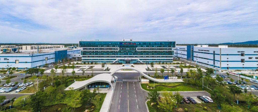
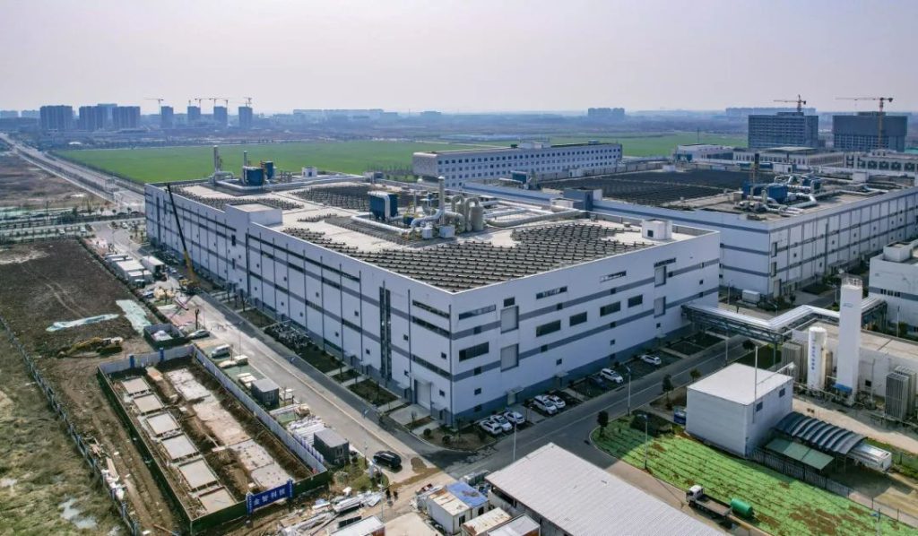
The project was settled in Pukou Economic Development Zone in September 2018, with a total project investment of 8 billion yuan, covering an area of 300 acres, officially put into production in July 2020, and realizing an output value of 222 million yuan in the year of 2020, 1.156 billion yuan in the year of 2021, 1.723 billion yuan in the year of 2022, and 2.5 billion yuan in the year of 2023 in terms of revenue. The product process includes BGA, LGA, DFN, QFN, FC, MEMS, Memory and other packages, of which BGA class packaging technology products, the domestic market share of 25%.
Up to now completed investment of more than 6 billion yuan, completed the construction of 300 acres, has built 206,000 square meters of plant.Introduced about 4,000 sets of process equipment, FC series products and BGA substrate series MEMS series products annual sealing measurement of nearly 5 billion.
02
Huatian Nanjing IC Advanced Packaging
Industrial Base Phase II Project

The total investment of the project is 10 billion yuan, the project site is about 188 acres, it is proposed to build 200,000 square meters of new plants and supporting facilities, and new introduction of high-end production equipment. The products of the project are located in the high-end packaging of resin substrate, and the packaging form is based on Chiplet/FCBGA/SiP, and the products will be mainly applied to storage, RF, arithmetic (AI), and automatic driving.
The project was officially signed on 3/28/2024.